Semiconductor
Here is a silicon crystal (= intrinsic semiconductor). Use the arrows or the small pictures below to keep track of what is happening.

Lattice of neutral Si atoms: 4 electrons in the last shells
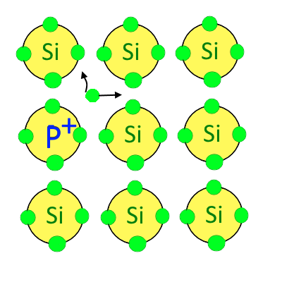
Doping: We integrate phosphorus atoms of the
→ V group with 5 electrons in the last layer (one too much for the perfect Si grille!)
These electrons are rejected by thermal energy in order to restore the perfect structure of the Si lattice.
These electrons rarely find back to their starting point.
They then circulate in a positively charged network: this is the N network.
Lattice of neutral Si atoms: 4 electrons in the last shells
Doping: We integrate boron atoms of the
→ III. Group with 3 electrons in the last layer (one too few for the perfect Si lattice!)
Thermal energy releases electrons from Si and leaves behind "holes".
These electrons find pass on boron atoms to try to recreate a perfect network with 4 electrons in the last layers.
The holes can be filled with electrons from other Si atoms. Then the holes "circulate": this is the P network.
.. if it is converted into an N-type semiconductor:


Lattice of neutral Si atoms: 4 electrons in the last layers.
.. and if it is converted into a P-type semiconductor:


Lattice of neutral Si atoms: 4 electrons in the last layers


